TSMC and Samsung Race Toward 1.4nm Chips — The Future of AI Performance
Last verified: 11 Nov 2025 (sources: TSMC press release, TrendForce, Reuters, industry press)
Executive Summary (TL;DR)
The semiconductor foundry race has moved beyond 3nm and 2nm into 1.4nm (often referred to as “A14” or 1.4nm-class) process technology. Taiwan Semiconductor Manufacturing Company (TSMC) and Samsung Foundry remain the two primary competitors. TSMC announced an A14 (1.4nm) program and trade reports indicate preparatory work for a new fab in Taichung; Samsung has signaled a pushback of mass-production timing for its 1.4nm node into 2028–2029 as it prioritizes 2nm yield stabilization. The technical shift is led by the adoption of gate-all-around (GAA) transistor architectures, continued reliance on EUV lithography, and system-level co-design that optimizes chips for AI workloads. These changes promise measurable gains in AI training and inference performance, lower energy per operation, and better on-device capability — but real market impact will depend on yield, supply, customer adoption, and ecosystem readiness.

Frequently Asked Questions (FAQ)
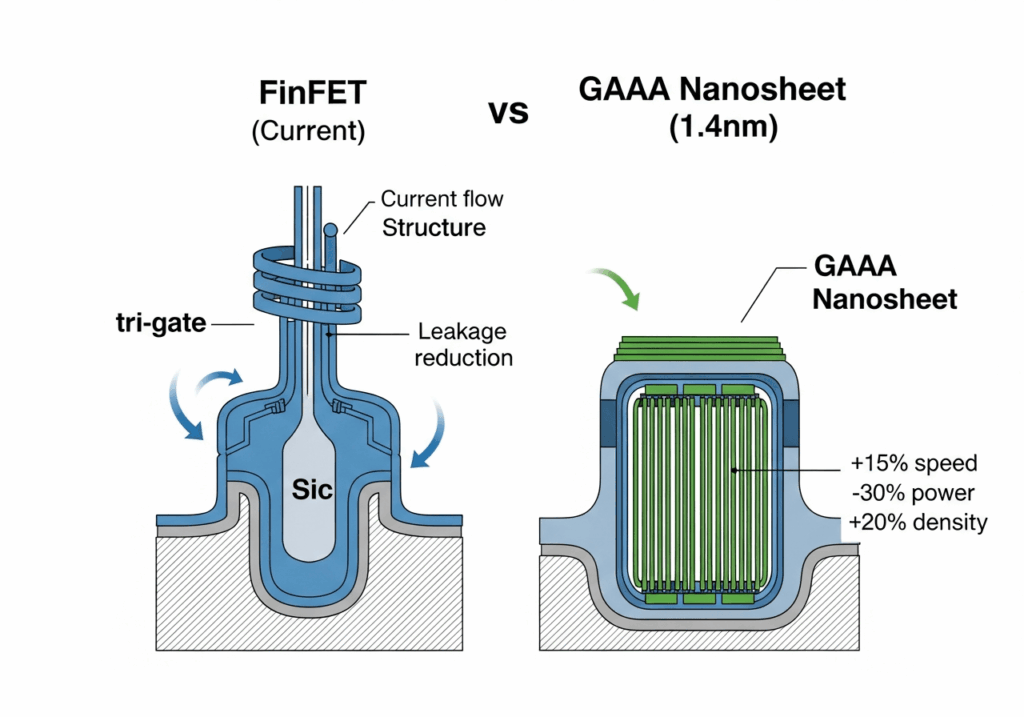
Q: What is 1.4nm chip technology?
A: 1.4nm chips represent the next generation of semiconductor manufacturing, using gate-all-around (GAA) nanosheet transistors to achieve higher performance, better power efficiency, and increased transistor density compared to current 3nm and 2nm processes.
Q: When will 1.4nm chips be available?
A: TSMC has announced plans for A14 (1.4nm) mass production in 2028, while Samsung has reportedly delayed its 1.4nm production timeline to 2029. (See sources below.)
Q: How much better are 1.4nm chips for AI performance?
A: According to TSMC’s A14 announcement, the company estimates up to 15% higher performance or 30% lower power consumption compared to 2nm, with 20–23% higher transistor density, which could directly benefit AI training and inference workloads. These are vendor-reported figures and should be treated as directional until independent benchmarks are available.
Q: Which company will lead the 1.4nm race?
A: TSMC currently appears to lead with announced 2028 production plans and reported foundry expansion investments, while Samsung focuses on perfecting 2nm before advancing to 1.4nm in 2029.
1. Why 1.4nm Matters for AI (and Why the Industry Cares)
AI workloads — especially large language models and generative models — strain both compute throughput and memory bandwidth. Improvements in advanced node roadmap transitions translate into:
- Higher transistor density: more compute elements and larger on-die caches per unit area.
- Better power efficiency: lower energy per operation means cheaper training runs and more practical edge AI.
- Higher clock/performance headroom: faster cores for inference and lower latency for real-time AI.
Improvements at the node level also compound with system design and advanced packaging — and will play a central role in cloud and enterprise systems, as seen in recent AI cloud infrastructure expansion led by OpenAI’s AWS partnership.
2. The Technical Picture — GAA, EUV, and What’s Changing
Two technical trends make the 1.4nm node feasible and useful:
Gate-All-Around (GAA) transistors
GAA replaces FinFET at extremely small nodes by surrounding the channel on all sides (nanosheets or nanowires). This provides better control of leakage and drive current, which is crucial for both energy efficiency and performance at tiny geometries. Samsung has publicly emphasized GAA in its foundry capacity expansion roadmap; TSMC also adopts nanosheet/GAA-class structures for its A14 designs.
EUV lithography (multiple generations)
Continued use of EUV tools is central — but the industry debate centers on whether high-NA EUV is required. TSMC has stated publicly that it does not plan to rely on High-NA EUV for its A14/1.4nm-class production, instead achieving gains through process innovation on current 0.33 NA EUV platforms and transistor design. That reduces dependence on scarce, costly High-NA machines and helps schedule volumes earlier.
3. TSMC: A14, Fab Construction and Performance Claims
Recent reporting and company statements show TSMC moving aggressively on the A14 (1.4nm-class) path:
Construction timeline
Trade reports and TSMC statements indicate the company planned to break ground on a new A14 fab in Taichung on November 5, 2025, with trial production targeting 2027 and mass ramping expected in 2028. Industry reports put the initial investment near US$49 billion for the site often described as Fab 25.
Performance specifications
TSMC’s A14 announcement (April 2025) claims notable performance and power improvements versus the 2nm class: the company estimates up to 15% higher single-thread performance or 25–30% lower power at iso-performance for A14 compared to N2 in some product classes, and roughly 20–23% increase in transistor density over N2 depending on cell libraries. TSMC reported these gains come from transistor architecture and cell-level innovation rather than an immediate need for High-NA EUV. Independent benchmarks will determine real-world results.
What to watch: yields at scale, customer tape-outs from partners (e.g., Nvidia’s AI chip demand), and whether TSMC’s A14 delivers projected performance across both accelerator and mobile classes.
4. Samsung: Roadmap Adjustments and Timeline Changes

Samsung’s 1.4nm strategy has undergone changes from its original aggressive roadmap:
Original timeline vs. reality
Samsung initially announced plans targeting 2nm by 2025 and 1.4nm by 2027. However, recent industry reporting shows the company has pushed back 1.4nm mass production into 2028–2029 — potentially two years behind earlier timelines.
Strategic refocus
Samsung appears to be pacing capital intensity to ensure higher-priority nodes (like 2nm) meet customer demand first. The company is doubling down on refining its 2nm process family while postponing broad investment in the 1.4nm node. Trade reports estimate Samsung’s SF2 yields have been improving (some reports cite 30–50% in mid-2025) with company targets of 60–70% by year-end.
What to watch: Samsung’s Pyeongtaek investments, customer commitments from Qualcomm and other partners, and public yield reports for 2nm/3nm — these signal when 1.4nm resources will materially scale. Samsung’s mobile and thermal work also connects to recent innovation in its Exynos line (see Exynos thermal breakthrough).
5. Realistic Performance Expectations (Numbers — Carefully Sourced)
Public and trade reports provide preliminary insights rather than absolute guarantees:
TSMC A14 vs N2 (2nm): TSMC reported A14 could offer up to 15% higher single-thread performance or 25–30% lower power at iso-performance for A14 compared to N2 in some product classes, and roughly 20–23% increase in transistor density over N2 depending on cell libraries. These are vendor-reported engineering claims based on internal benchmarks and process modeling.
Samsung’s projections: Samsung’s roadmap materials (2022) targeted similar performance improvements for 1.4nm, but timing and real-world results depend on subsequent yield and process maturity. Recent reporting indicates Samsung has adjusted investment timing for its 1.4nm development to 2029.
Author’s note: transistor-level metrics and percentage improvements differ across workloads (mobile CPU vs GPU/accelerator vs NPU). Treat vendor numbers as directional estimates. Always check vendor datasheets and independent benchmarks when available.
6. Market and Ecosystem Implications for AI
For hyperscalers and AI infrastructure providers like Nvidia, Google, Microsoft, and Amazon: better efficiency reduces cost per training token and allows higher throughput per rack — direct OPEX benefits.
For chip designers (NPU/accelerator vendors): higher density enables more accelerator cores and larger on-chip SRAM, improving model parallelism and reducing off-chip memory bottlenecks.
For mobile & edge markets: improved per-watt performance lets OEMs run larger models locally (privacy/security wins) and reduces thermal throttling.
For investors and supply chains: company execution (fab completion, yield curves) becomes the central risk factor. Early technology leadership confers both premium foundry pricing and long-term customer lock-in.
For macro context, monitor how semiconductor advances interact with the broader AI market impact and policy changes impacting capital flows.
7. Who’s Ahead — A Balanced View
| Aspect | TSMC | Samsung |
|---|---|---|
| 1.4nm Timeline | 2028 production (announced) | 2029 production (reported) |
| Investment | ~$49B reported (Fab 25) | Delayed pending 2nm success |
| Technical Approach | 2nd Gen GAA, no High-NA EUV | GAA-focused, timing TBD |
| Current Status | Reported fab construction | Focusing on 2nm yields |
| Competitive Edge | Proven execution, customer base | Early GAA adoption, integration |
Bottom line: leadership will be decided by the combination of process performance, realized yield at scale, and customer tape-outs — not just roadmap announcements.
8. Risks, Unknowns, and What Could Change the Picture
- Yield curves and ramp speeds: even if technical claims hold in lab benches, the cost and time to reach high yields can delay commercial advantages.
- Equipment availability: future node refinements might require additional lithography capabilities.
- Customer design timelines: big customers (e.g., Nvidia, Apple) decide which node to adopt based on performance and time-to-market.
- Geopolitics and subsidies: CHIPS acts and national funding can reshape capacity decisions and speed up or slow facility builds.
- Alternative approaches: chiplets and advanced packaging can blunt the urgency for single-die density improvements by scaling performance via packaging.
9. Practical Advice for Businesses and Technologists
AI infrastructure buyers: plan for staged upgrades. Expect meaningful gains in 2028–2029 for A14 accelerators; negotiate supply commitments early.
Chip designers: maintain multi-node support and consider chiplet strategies to shorten time-to-market.
Edge device designers: evaluate model quantization and pruning together with hardware gains — node improvements complement model optimization, they don’t replace it.
Investors: watch tape-outs (customer announcements), yield disclosures, and capital spending — those are leading indicators of real production capability. Also monitor the evolving AI policy landscape which can influence capital allocation and strategic national priorities.
10. Detailed Source Citations
This article was compiled from primary and reputable trade and industry reports, cross-checked against recent company announcements and technical analyses.
- TSMC A14 process & performance claims — TSMC official press release, April 23, 2025
- TSMC fab construction & investment reports — TrendForce industry analysis, 2025
- TSMC High-NA EUV stance — Tom’s Hardware coverage, May 2025
- Samsung timeline delay reports — TrendForce reporting, 2025
- Samsung 2nm yield target reporting — Wccftech industry coverage, 2025
Legal Disclaimer
The information in this article is based on public reports, industry statements, and trade analyses available at the time of writing (research verified against sources published in 2022–2025). Roadmaps, production timelines, and performance claims referenced are forward-looking and subject to change due to technical, commercial, or geopolitical factors. Vendor-reported performance figures are estimates based on internal modeling and may differ from real-world results. This article is for informational and journalistic purposes only and does not constitute investment advice. Readers should verify specific technical claims with vendor datasheets, official press releases, and independent benchmark results before making purchasing or investment decisions.
© [Sezarr Overseas News] — Published: 2025-11-11 · Last verified: 2025-11-11
Sezarr
The founder of Sezarr Overseas, sharing insights on global business trends, investment strategies, and the future of technology. Passionate about empowering entrepreneurs and investors with data-driven analysis.